"As I recall, those two chips were fairly large. And fairly late -- to the marketplace. We had lots of issues with them. [...] Sometimes the elegant solution isn't the best solution." -- Dave House, digressing to the 8271 during "Oral History Panel on the Development and Promotion of the Intel 8080 Microprocessor" [link], April 26th 2007, Computer History Museum, Mountain View, California.
Introduction
Around 1977, Intel released a floppy disc controller (FDC) chip called the 8271. This controller isn't particularly well known. It was mainly used in business computers and storage solutions, but its one breakthrough into the consumer space was with the BBC Micro, a UK-centric computer released in 1981.
 |
| Intel 8271 (left) in an issue 3 BBC Micro model B |
There are very few easily discovered details about this chip online, aside from the useful datasheet. This, combined with increasing observations of strange behavior, make the chip a bit of an enigma. My interest in the chip was piqued when I accidentally triggered a wild test mode that managed to corrupt one of my floppy discs even though the write protect tab was present! You can read about that here:
A wild bug: 1970s Intel 8271 disc chip ate my data!
Can we reverse engineer a detailed understanding of how it works? What wonders will we find?
Credits
The work described here represents the efforts of a virtual team that came together in an impromptu way to investigate the chip. There are many critical players, and special thanks go to:
- Nigel Barnes. Bridged the MAME community and BBC Micro community, locating someone with chip decapping skills.
- BeebMaster. Provided a couple of sacrificial 8271 chips for decapping.
- Sean Riddle. Decapped the chips and provided beautiful hi-resolution images.
- ZXGuesser, Diminished. Hardware level reverse engineering, including accurate extraction of ROM bits.
- Ken Shirriff. Provided notes on silicon macro structures, and located historic documents of great utility.
- Rich Talbot-Watkins, Chris Evans (me). Calculating the ISA, disassembling the ROM.
The beauty of the beast: recap and decap
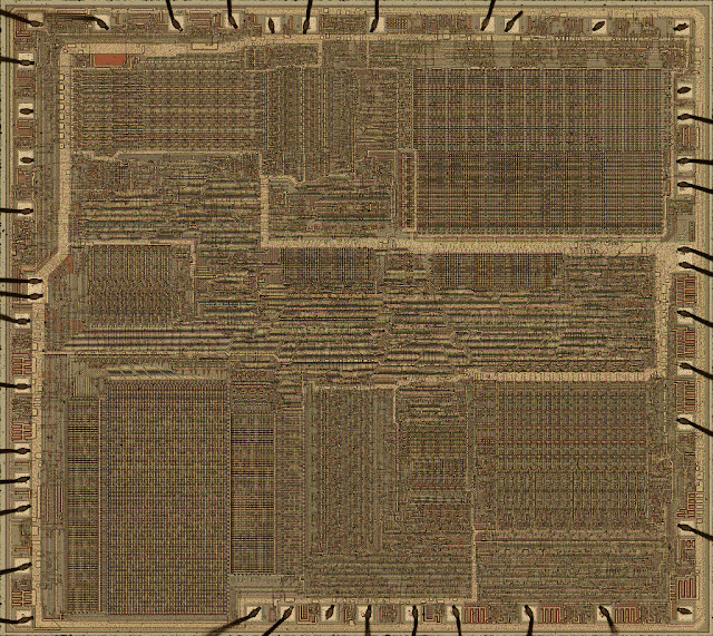
So to recap: we had a few indicators that this could be a very interesting chip. These range from the crazy test mode we found above, to the fact the data sheet hints at a large number of internal registers, with only a few documented.
And, to decap:
 |
| (See references at the end for very high resolution shots) |
This a complicated chip for an FDC! There are a large number of large structures present, densely packed. To illustrate the point, we can compare this chip with the heart of the BBC Micro -- a venerable, legendary 6502, as used in iconic 80s machines and consoles such as the Apple ][, Commodore 64 and NES:
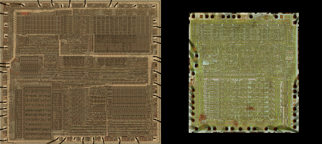 |
| 8271 left, 6502 right |
Not only is the 8271 larger than the main CPU by a significant amount, it also cost more by all accounts:
"In Acorn's wisdom, they had chosen the Intel 8271 disk controller for the BBC Micro - this controller was probably obsolete even before the BBC Micro was launched. The Acorn disk upgrade comprised the 8271, a handful of standard TTL ICs, an Acorn DFS ROM, and the disk manual. The ICs plugged into unpopulated sockets on the motherboard.
A few hardy folks tried sourcing the parts separately - which was fine, except that an 8271 tended to cost about £109 on its own, if you could find one..." -- [source link]
By contrast, the 6502 allegedly cost around $7.45 in 1981, which is a huge difference factor.
Getting the ROM bits
From a quick eyeball of the 8271 die, there are plenty of PLA-like structures, but perhaps most promisingly, a large rectangle of ROM in the lower left. Right away, we're thinking that this could indeed be a general purpose microcontroller CPU if there's a ROM program. Initial focus fell immediately to extracting the ROM.
ZXGuesser and Diminished put in a Herculean effort, transcribing the ROM bits first by hand and later with some tooling assist and cross-checking. In case you're wondering what transcribing ROM bits by hand looks like, it looks a little like this:
 |
| Look closely; those cyan annotations are 0s and 1s! |
The ROM matrix is 64x108 bit cells, for a ROM size of 864 bytes.
Once you've gotten the ROM bits, you still have the challenge of assembling them together into a correctly sequenced byte stream. This isn't always as easy as you might think, and is particularly rough when you don't have a reliable way of telling if the extracted bytes are ok, as is the case here. During my research, I found:
- Two 8-bit bytes interleaved.
- Bits and bytes heavily interleaved in a Channel F game cartridge.
- Byte ordering permuted fairly arbitrarily -- obfuscation?
Fortunately, the ROM reversers also looked at the row and column circuitry connecting the ROM, and gave a fairly robust opinion that the ROM bits / bytes are:
- Left-to-right, top-to-bottom.
- Bits inverted relative to the initial decode in the image above.
- Bits MSB first.
- Bytes build from 1 bit per linear 8 bit group.
Architecture hints
As Rich and myself engaged in efforts to try and disassemble the ROM, without any prior knowledge of the Instruction Set Architecture (ISA), I was fortunate enough to have a conversation with Ken Shirriff (righto.com) about this interesting chip. Against all odds, he found a detailed conference presentation abstract from 1977 [link to copy of full abstract].
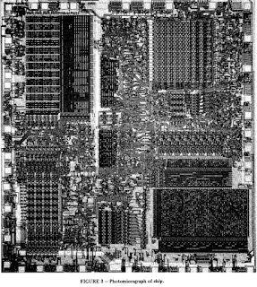
This image from the abstract, will look familiar (imagine +90 degrees rotated).
"A DUAL PROCESSOR microprogrammable chip that implements a specialized architecture for high-speed serial data controllers will be described. The chip measures 218 mils by 244 mils and contains 22,000 transistors..."
22,000 transistors!! We knew this was a bit of a chonker, but for reference, the 6502 has 3,218 transistors; the 8080 6,000 transistors and the 8086 29,000 transistors. Yes, the 8271 is not that far off an 8086 in terms of transistor count.
This instructive table and diagram are also from the abstract:
This confirms our suspicions that we are dealing with a general purpose CPU, coupled with some acceleration for I/O. The general purpose CPU has the features you'd expect, including a PC, stack, ALU, accumulator, registers, and access to a bus. Further detail in the abstract includes "32 eight-bit registers" and "four-level stack".
The presence of a a bit processor (a co-processor if you like) with 250ns cycle time resolves the elephant in the room with the "general CPU" theory. A general CPU of the era probably wouldn't be fast enough to calculate CRC16 at the disc data rate. However, a specialized PLA-driven bit engine bolted on to the side will do just fine.
Finally on this abstract, we see that it states "To date, two distinct controllers have been microprogrammed: a floppy disk controller and a synchronous data link controller (SDLC)". Well, we've found the FDC, the 8271. Intel's SDLC from the era was the 8273. Enter Sean Riddle once more -- what a star -- and another sacrificed chip or two later, we have our result:
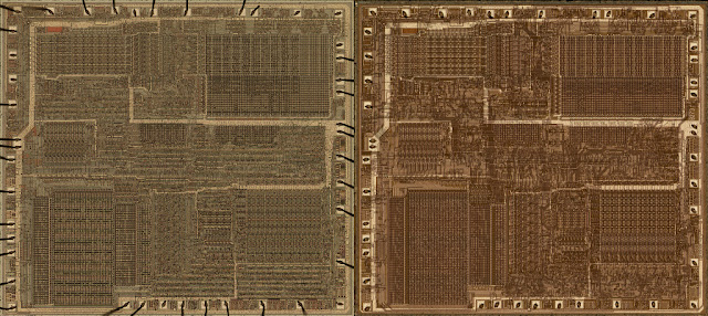 |
| 8271 left, 8273 right |
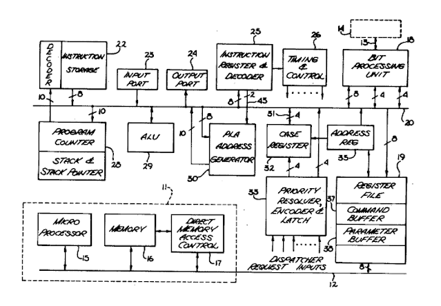
Ken also found a patent relating to this dual core design! It's US4152761. [link to a more complete version]. There's a lot of useful architectural detail in the patent, including this interesting summary of key components.
 |
| From US4,152,761 |
As can be seen, there's additional complexity described here that falls outside what we'd expect from a traditional CPU. There's dispatcher requests, priority resolution, a "case" and an "address" register in addition to the program counter and instruction register. This relates to some form of scheduling, which we'll encounter later.
Finally, here's a diagram (courtesy of Ken). It's an early estimation of how the architecture we've seen in the the documents so far might map to the silicon. As a dual processor behemoth, note how there's two ALUs, two sets of registers, lots of PLAs (including a couple to the left and right of the "control" label), and plenty of patches of silicon with unknown function.
From bits to bytes to an Instruction Set Architecture (ISA)
With an overview of the architecture, we have a better idea of what sort of opcodes we might find in the instruction set. The more pieces of the puzzle we have in our heads, the better chance we have of making abstract connections in our attempt to solve a problem with a lot of moving parts.
Initial attempts to disassemble the ROM centered around the theory that the CPU core might be based on the Intel MCS-48 microcontroller series. This series includes the well-known 8048 and has several variants such as the slightly cut-down 8020 (less I/O lines). And why wouldn't this core be based on a further cut-down 8020? It just fits too well: 1K ROM, 64 registers, 13 I/O lines. The timing works well too: the MCS-48 series first launched in 1976, making the core available before the release of the 8271. So the theory went, you'd be crazy as an 1970s Intel employee to not just walk down the corridor and raid the parts bin of your colleagues in order to get a headstart.
The MCS-48 theory turned out to fit extremely well.... but be false. No amount of ROM bit / byte wrangling led to sensible MCS-48 disassemblies.
Back to the drawing board, we looked again at our "probably correct" ROM decode and analyzed it for patterns we'd expect to find in an 8271 ROM, based on our understanding of how the controller works, and how disc recording works in general. Here's a section we found enlightening:
Most significant is the appearance of the constants $FE + $C7 (middle box), then $E5 + $FF (lower box) in a the same context. These constants are the data byte + clocks byte we'd expect to see in the format routine for FM (single density) formatted discs. $FE + $C7 is the sector header marker, and $E5 + $FF is the default fill byte for freshly formatted sectors. As a bonus, we speculated that $E9 (appearing four times in a row) could be a shift left or right opcode, with $FD perhaps being RET. All in all, some strong circumstantial evidence for a correct decode.
After the MCS-48 opcode list failed to match our ROM, we spent a long time trying to derive an alternate instruction set.
But it's hard; it's a bit like one of those jigsaw puzzles where every piece is the exact same color. It's very hard to find a start as there are so many different possibilities to try. Research is too often presented as a neatly packaged result, with no mention of the struggle. I think this contributes to discouraging newcomers. So make no mistake: this was a struggle; it went on for some time; there was swearing; and the characteristics leading to success were perseverance and grit as opposed to any particular technical ability.
The breakthrough was catalyzed when the hardware investigations got a good read on the wiring and content of one of the instruction PLAs associated with the byte processor. The PLA in question is actually the darker rectangular block to the left of the "control" label in the image above. It is populated like this:
 |
| Thanks to Diminished! |
With the instruction PLAs decoded, it would be possible to trace the effects of each 8-bit opcode by following activation lines to the registers, stack, ALU, etc. However, we were able to hit our breakthrough with only opcode ranges, provided by this PLA. Of specific interest is these ranges from Rich:
1111 1100 FC1111 1101 FD[...]0010 xxxx 20-2F[...]0011 xxxx 30-3F[...]001x xxxx 20-3F
The specialized $FC and $FD match our theory of CALL and RET, but more pivotal is the range of $20-$3F, split into 2x 16 wide blocks. Immediately, I speculated this could be "move register to accumulator" and "move accumulator to register". This would turn out to be correct. Furthermore, I noted that opcode $0? was common before $2? or $3?, e.g.
05D: 04 22 03 35
This led to the theory that these are register bank selection opcodes. Similar to the MCS-48, the theory is that there aren't enough opcodes for all operations to be able to reference all 32 registers, so there must be a bank select. This also would turn out to be correct. In fact, with these pieces, the jigsaw started to fall in place, and fall into place faster and faster.
Some ROM code examples
For these code examples, bear in mind that the Instruction Set Architecture (ISA) presented here hasn't seen public light of day as far as we know. We've had to invent our own assembly mnemonics, although they're designed to be familiar to anyone familiar with assembly languages in general. Some specific notes:
- SEL RB is SELect Register Bank, and provides the base index for register access (multiply by 8 to get actual index).
- Note that all register references are by index, not register number. A register number can be calculated with the index and register bank.
1) READ SPECIAL REGISTER
32E 00 SEL RB 0
32F 27 MOV A, I7 ; R7 ($07) (param 1)
330 30 MOV I0, A ; R0 ($00) = register index
331 F8 MOV A, [I0] ; read special register value to A
332 02 SEL RB 2
333 36 MOV I6, A ; R22 ($16) (ext RESULT) = A
334 0E SEL RB 14
335 EE SYS 2, RB ; JMP (2,E,0) => $288, .post_command_tidy_up
The READ SPECIAL REGISTER command is one of the simplest. As suspected, "special register" externally is just "index into the 32 registers" internally. We can also note plenty of interesting things:
- The command setup code, which we'll see in a bit, writes parameters to R7 downwards.
- Indirect reads and writes are done via special opcodes that indirect through I0 (typically but not always R0), as per the MCS-48 architecture.
- Some of the internal registers interact with the external bus registers used to interact with the host CPU. R22 is where you write values for them to appear in "ext RESULT", which is read with BBC Micro's 6502 at memory location $FE81.
- The "register bank" concept appears to be re-used to provide a lookup index to the SYS 2, RB opcode. You might consider this a minor kludge.
- In order to jump from page 3 ($3??) to page 2 ($2??) at the end, a special SYS opcode is required. Normal JMP / CALL instructions only have an 8-bit operand and can only jump to the current page. SYS opcodes look up a 10-bit PC from a hard coded table.
- The command exits by jumping to a common exit routine, .post_command_tidy_up. This routine disables most of the chip, including the bit processor, and events. This will be important later.
2) SPECIFY
066 00 SEL RB 0
067 27 MOV A, I7 ; R7 ($07) (param 1)
068 30 MOV I0, A ; R0 ($00) = destination index
069 F1 03 MOV I1, #$03 ; R1 ($01) = count of 3 extra parameters
06B 14 YIELDTO 4 ; seems to set PARAM callback to
; .wakeup_PARAM_4_SPECIFY, then YIELD
; ** entry point (3, segment 9, routine 4 5 6 7 C D E F)
.wakeup_PARAM_4_SPECIFY
06C 03 SEL RB 3
06D 2E MOV A, IE ; R30 ($1E) (ext PARAM)
06E 00 SEL RB 0
06F E8 MOV [I0], A
070 00 SEL RB 0
071 80 INC I0
072 A1 DEC I1 ; R1 ($01), decrement count
073 8A 8C BZ $08C ; branch if done
; lands at SEL RB 14, JMP RB
; which jumps to .post_command_tidy_up
075 FF YIELD
- SPECIFY accepts and applies the register writes immediately, YIELDing (sleeping / idling) between writes and waiting for the host CPU to supply the next register. This means the SPECIFY command might be partially completed for some time, and never fully completed, depending on how we program the chip. This will be significant later.
- SPECIFY internally uses R0 as a destination index to write register values, and R1 as a count to complete. This makes it an ideal candidate to do some black box testing to confirm the chip behaves the same as our source code disassembly. Specifically, I tried and confirmed:
- Pass the first parameter to SPECIFY as 0, indicating we are writing register values starting at R0. Note that as per the code, R0 is used internally by SPECIFY.
- Pass the second parameter as $22. This will get written to R0 (because R0 currently points to R0) and incremented, leaving $23 in R0. This has "corrupted" R0.
- Pass the third parameter as $48. This will get written to MMIO register R35 ($23), and should turn on the drive motor.
- Do not pass a fourth parameter. Despite not “completing” the full four parameters of the command, we expect the writing of the third parameter to have the effect as just described. It does on real hardware.
- For commands other than SCAN and FORMAT, the number of parameters expected is actually encoding in to the low order bits of the command byte. Undoubtedly, this saves space in the ROM. This is another case where a simple test can confirm the behavior claimed by the ROM code:
- Take a command that takes 1 parameter, e.g. READ SPECIAL REGISTER.
- Increment the command byte and supply that to the 8271 instead.
- We'd expect the 8271 to require 2 parameters to start the command, but then ignore the second parameter and behave as if the 1 parameter version was used. This is indeed observed on real hardware.
Javascript on a (1970s!) chip
- YIELD. $FF. This instruction tells the processor to switch to running the highest priority dispatcher request, or (more likely) go idle if there's no dispatcher request active.
- TASK t, r. $B8-$BF, 2 bytes. This instruction changes the callback routine for the specified task. Callback routines are specified as an integer that form part of a lookup key into a table of ROM addresses.
- YIELDTO r. $10-$1F. Change the callback routine for the currently executing task and yield.
- SYS 0, RB, A. $EC. Jump to the ROM address at key (0, RB, A) in the address PLA. RB is the current register bank from the SEL RB instruction, and A is the accumulator value.
- SYS 1, RB, R. $ED. Jump to the ROM address at key (1, RB, R) in the address PLA. RB is the current register bank from the SEL RB instruction, and R is current routine value.
- SYS 2, RB. $EE. Jump to the ROM address at key (2, RB, 0) in the address PLA. RB is the current register bank.
- PC == $035
- TASK == 4
- SEGMENT == 9, ROUTINE == 1
- 0: Not reversed at all. Appears to be related to the SCAN command, which isn't enabled on the BBC Micro due to lack of DMA.
- 1: Bit processor event, e.g. found sync, lost sync, CRC error.
- 2: Bit processor, read byte ready.
- 3: Bit processor, write byte needed.
- 4: External parmeter register written.
- 5: appears unused. (Could be permanently connected to external command register?)
- 6: Disc drive index pulse.
- 7: appears unused.
Unusual features of the ISA
Interface to the bit processor
 |
| Registers 0-63, read on a real BBC Micro, illustrating mirroring of the bit processor registers |
- 0: control register, 4 bits
- Bit 0 (0x01) => gather CRC (?)
- Bit 1 (0x02) => finish CRC (?)
- Bit 2 (0x04) => 1 for read, 0 for write
- Bit 3 (0x08) => idle state
- The generic command entry code corrupts bit processor state on entry.
- The generic command exit code resets the bit processor and associated callbacks on exit (but strangely and usefully not for WRITE SPECIAL REGISTER).
- The latency of WRITE SPECIAL REGISTER is terrible.
Writing the unwritable
- The internal command register itself is corrupted, i.e. mismatched with the currently executing command. It is referenced from time to time so this may be useful to us.
- The illegal command will change internal register values, which may impact the execution of the current command.
- The illegal command may change or disable callbacks, or reset or reconfigure the bit processor.
- Formatting a track with a single sector header.
- Issue a WRITE DATA command for that sector, of size 8192 bytes. A track is only 3125 bytes (with a perfectly calibrated drive), so:
- At the first wrap around, start writing the track of bytes we want.
- 3125 or so bytes later, at the second wrap around, abort the command by resetting the controller.
- The SPECIFY command was used instead of WRITE SPECIAL REGISTER to help with latency concerns. The SPECIFY command can be "primed" by passing the command and the first parameter, such that the second parameter (first register value to write) executes the write and executes with low latency at just the right moment.
- The WRITE SPECIAL REGISTER command exits without resetting the bit processor or clearing all the I/O callbacks. Unfortunately, the same cannot be said for SPECIFY. Fortunately, we don't have to exit the SPECIFY command! It starts having the useful side effect of writing internal registers before it is complete. And then you can later restart it again and again, never completing it.
- The act of command dispatch corrupts the MMIO clocks byte register! This is very unexpected but it uses MMIO R36 as a temporary storage location while it is calculating which disc drive (0 or 1) is selected, and whether it changed. It is worth looking at:
The line in orange is the one in question. I annotated it as iffy with ??? when I first disassembled it as it looked wacky. But, it's correct and a real machine exhibits the corrupted clocks precisely as described by the code. The corrupt clocks value, $40 if writing to drive 0, is shown in orange in the above diagram. Once you know it's there, and why, the easiest way to navigate around it is to arrange for the clocks corruption to land where it doesn't case problems. When paired with a $FF data byte, it doesn't create weak bits on the disc surface, and the controller actually seems to skip over it on read.
- The write I/O path, by some stroke of good fortune, resets the clocks byte to $FF on every write I/O callback. This saves us a lot of trouble:
- Careful timing is needed. There's a pipeline of bytes from the external data register to the internal bit processor data byte register to the actual output pulse machinery. This needs to be accounted for.
Other successes and failures
- beebjit now has a much more accurate 8271 driver.
- Unexplained weirdness trying to read a sector with logical track id $FF has been explained as an integer overflow in the bad tracks handling.
- Sectors on a non-zero physical track, but with a zero logical track id, were believed "impossible" to read. I'm able to read them by using the "command within command" trick. Once a READ DATA command is safely underway, including having processed the seek request and gone idle, it's possible to use WRITE SPECIAL REGISTER to change R7 (command param 1, which is the requested track) to zero, and have the sector read fine. The issue is that references to logical track 0 in the seek code are always treated as a mandate to find physical track 0. You need to bypass that.
- Reading or writing MFM (double density) -- looks fundamentally impossible. Does not appear to be a capability in the hard-wired bit processor.
- Executing arbitrary code on the chip. This is a shame, as the byte processor is a capable CPU! Who knows what we could use a little co-processor for? Things making this hard include:
- Separation of code and data in separate address spaces.
- No references to the stack possible outside of CALL and RET.
- Indirect jump targets stored in a read-only PLA. (Microsoft CFG? :)
- ... and yes, curiously, these accidental defenses all sound similar to defensive technologies investigated or deployed since year 2000. So, the 1970s called and...
Summary
The 8271 has exceeded our expectations! Where to start? It's a massive chip, encompassing dual cores and a Javascript like execution model. Remember, this was the mid-1970s. Its general purpose CPU runs an Intel instruction set architecture that I don't believe has been publicly documented until now. It's not every day we get the treat of a new Intel ISA.
We never got to the bottom of the crazy test mode that started this whole investigation. There's no trace of it in the byte processor ROM, so it must be handled by some other component on the silicon. Something to investigate for another day perhaps.
Having seen the complexity of the chip, I must confess to a feeling of surprise every time my BBC Micro successfully loads a disc.
Epilogue
Given the 8271 issues with cost, heat, supply chain, complexity, and lack of MFM, it wouldn't be surprising if Intel had had enough with the architecture behind the 8271 and 8273. Intel staggered bravely forward with the 8272, which introduced MFM support and... hang on, let's have a look at a decapitated one of those...
 |
| Left to right: Intel 8271, NEC D765, Intel 8272 |
This is very cheeky! The 8272 die may say "8272 (c) Intel 1979" but it is the same die as a NEC D765, stamped "NEC D765B". It looks like Intel may have licensed the NEC design. The NEC doesn't appear much smaller in terms of die size, but the layout looks much simpler and less busy. Bizarrely, Intel appears to have fabbed the 8272 much larger than the NEC.
Extra references
- StarDot forum thread where the investigation unfolded: [link]
- Sean Riddle's decap page: [link]
- beebjit's 8271 driver: [link]
- 8271 tests and tools (warning: rough) for the BBC Micro: [link]
- Live document for 8271 disassembly: [link]
- Very high resolution die shots of the 8271 and 8273 (beware, will hang browsers!): [link]

